
onsemi (Ansemi)
画像はイメージの場合もございます。
商品詳細は仕様をご覧ください。
商品詳細は仕様をご覧ください。
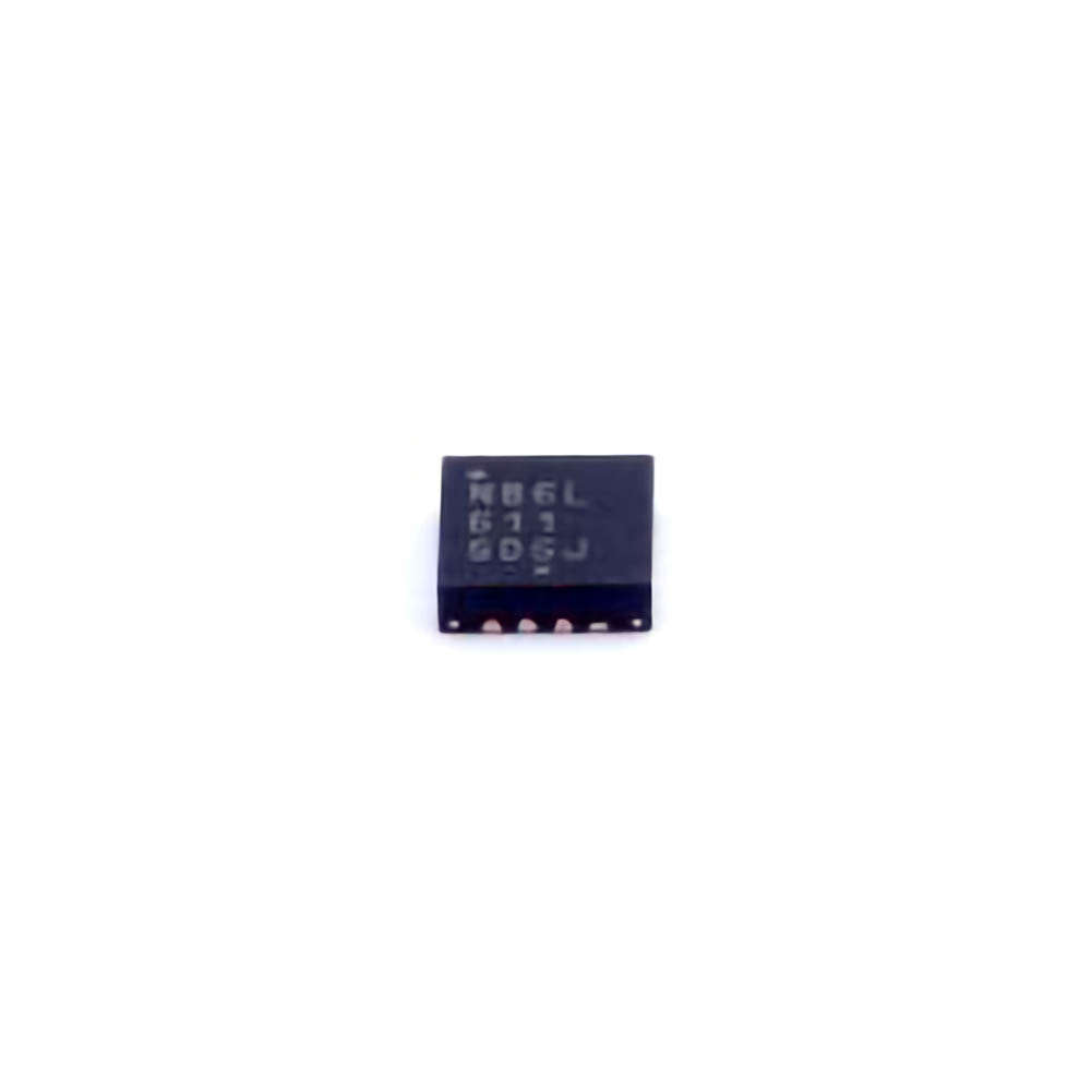
NB6L611MNG
2 differential, 3 GHz / 2.5 V / 3.3 V with LVPECL output
部品番号
NB6L611MNG
カテゴリー
RTC/Clock Chip > Clock Buffer, Driver
メーカー/ブランド
onsemi (Ansemi)
カプセル化
QFN-16-EP(3x3)
パッキング
Tube
パッケージの数
123
説明
The NB6L611 is a differential 1:2 clock or data fanout buffer. The differential inputs incorporate internal 50 Ω termination resistors accessed through the VTD pin and accept LVPECL, CML, LVDS, LVCMOS, or LVTTL logic levels. The VREFAC pin, the internally generated supply voltage, is provided only for this device. VREFAC is used as the reference voltage for single-ended PECL or NECL inputs. For the single-ended input case, the unused complementary differential input is connected to VREFAC as the switching reference voltage. The VREFAC also couples the capacitor to the input rebias. When used, decouple VREFAC with a 0.01 µF capacitor and limit source/sink current to 0.5 mA. When not in use, the VREFAC output should be left open. The device is packaged in a small 3mm x 3mm 16-pin QFN package. NB6L611 belongs to the ECLinPS MAX series of high-performance clock and data management products.
リクエスト引用
必須フィールドをすべて入力し、送信をクリックしてください。12 時間以内に電子メールでご連絡いたします。何か問題がございましたら、メッセージを残すか、[email protected] まで電子メールを送信してください。 できるだけ早く対応させていただきます。
在庫あり 77241 PCS
連絡先
関連製品

のキーワード NB6L611MNG
NB6L611MNG 電子部品
NB6L611MNG 売上
NB6L611MNG サプライヤー
NB6L611MNG ディストリビュータ
NB6L611MNG データテーブル
NB6L611MNGの写真
NB6L611MNG 価格
NB6L611MNG オファー
NB6L611MNG 最安値
NB6L611MNG 検索
NB6L611MNG を購入中
NB6L611MNG チップ